In this section, we will look at digital inputs, and how we might use them to control digital outputs.
We will be using a simple “push-to-make switch” to generate a single digital bit of data.

Activity 3.1 – Simple Switch Input
Remember that a single digital signal is either ON or OFF. Numerically, we represent this as 1 or 0 (a single binary digit). The simplest way to generate a single bit input signal is with a push switch (shown below). The schematic to generate a digital input is as follows.
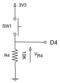
Wire up this circuit on your prototype board.
Activity 3.2 – Reading Digital Inputs
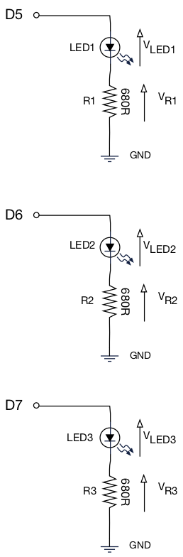
Wire up 3 LED’s as shown here. These will be used for outputs.
For this task, we are going to read the digital input using software. The objective is as follows:
When the user depresses a button, the red LED switches ON and stays ON (until the system is reset).
Remember – the input is connected to D4.
Maybe unsurprisingly, we use a component called a DigitalIn.
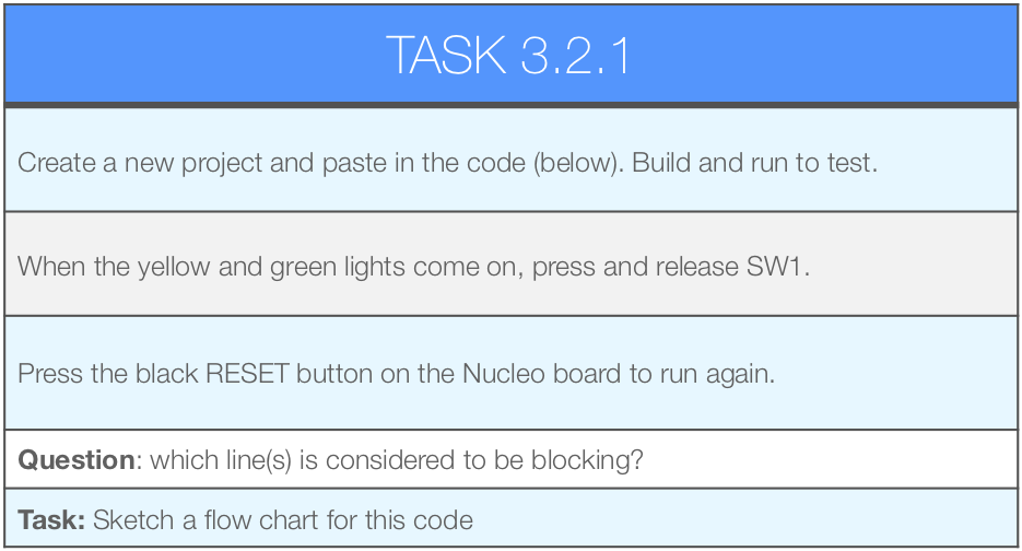
#include "mbed.h"

DigitalOut  red_led(D7);
DigitalOut  yellow_led(D6);
DigitalOut  green_led(D5);
DigitalIn   SW1(D4);

int main() {

    //Switch on Yellow and Green to indicate
    //that the code is running
    yellow_led = 1;
    green_led = 1;
    red_led = 0; //Set RED LED to OFF

    // Wait for SW1 to be pressed
    while (SW1 == 0) { }

    red_led = 1;	//Turn ON LED

    while (1) { }		//Repeat forever
}
Under the hood, there is a significant amount of work going on to set up the hardware in the right mode. The specifics are also vendor / board dependent.
We benefit greatly from hardware abstraction provided by the mbed C++ classes DigitalIn and DigitalOut. mbed provide identical interfaces for all supported mbed compliant boards. This is an example of a device driver.
Once again, we use of the the component from mbed to make interfacing with hardware simple.
DigitalIn SW1(D4);
where SW1 is an instance of DigitalIn, which can read pin D4. A critical line in this code is as follows:
while (SW1 == 0) { }
While the digital input SW1 is equal to zero, this code blocks the CPU in a tight polling loop. This is also known as spinning. This is NOT power or CPU efficient. Once the switch is pressed, an attempt to read SW1 will return a 1 and so the CPU will unblock.
It is not always bad practise to monitor peripheral hardware this way. If delays are likely to be very short, it can even have some advantages. However, the time between switch presses is indeterminate in this case, so spinning becomes wasteful of CPU time and most of all, power.
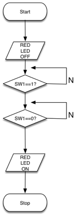
You might have found this to be an unreliable solution (depending on how clean the switch contacts are). In the next section, we will remind ourselves about “switch bounce” and how to avoid it as this added some additional complexity to our software.
Real World Signals
When working with physical hardware, both hardware and software engineers can take steps to reduce the probability of an erroneous input. In almost every case, errors are probabilistic. You can never engineer the probability to zero (ok, philosophical point maybe, but often it’s a very real issue).
As engineers, we have to recognise and mitigate against such failures, and at least know the probability and impact of failure that risk can be managed. Many systems are not fully autonomous, where human operators follow a protocol that is designed to monitor, manage and mitigate against risk.
A consumer gadget can accept a higher chance of failure than a safety critical system such as an anti-lock braking system or fly-by-wire system in a commercial aircraft. Some medical devices have to work with small and noisy signals from the human body, and have to use sophisticated mathematics and software to manage the error.
Switch Bounce
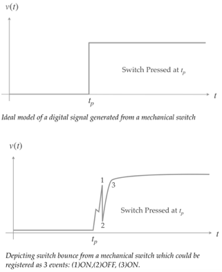
The reality is that mechanical switches are not perfect. Most switches suffer switch bounce to some degree. As you can see in the second diagram opposite, the waveform is not a perfect step like the ideal.
There are two common phenomena we much consider:
Noise – random signals superimposed on top of the waveform
Reactive effects – if you’ve not covered reactance (maybe you’re a computer science student), it should suffice to say that perfect step waveforms are almost impossible – signals often rise as an exponential curve (although it might be very rapid)
This reinforces the points that electronics is ultimately analog and signals are rarely ideal.
A problem with such phenomena is that their occurrence is stochastic (random, probability based). An engineer must be mindful of such issues, and design systems to minimise the probability of such events occurring or causing malfunction, especially in safety critical systems.
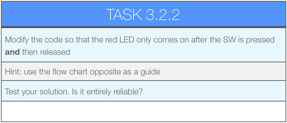
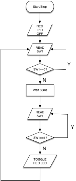
In the case of switch bounce, the exact nature is highly unpredictable. Consider the revised flow-chart below. This has added a delay after the first press is detected.
Adding the delay makes the system less responsive. This is often referred to as latency. This task illustrates some key points:
- electronic signals are rarely “ideal”
- switch inputs suffer “switch bounce”
- we sometimes have to make trade-offs, such as latency for reliability.
Non-Blocking Polling
A technique to read data from multiple input sources without blocking a thread of execution.
In the figure below, each device is polled to see if it has any available data (or if there has been any change). If yes, then the value is retrieved and stored. The next device is then polled.
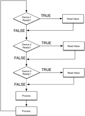
This method is an improvement over the busy-wait approach as it does not block the “thread” of execution, so all devices are queried at (typically) high rates.
This method does have some disadvantages however. The loop must repeat fast enough to read all devices before data is lost. This again means CPU cycles and power are being consumed even where there is no new input to process. Furthermore, the presence of conditional statements (if/while/switch) means the execution path through the code will vary, and thus the loop timing is likely to jitter. This can cause problems where data must be read at fixed intervals (as we will discover later).
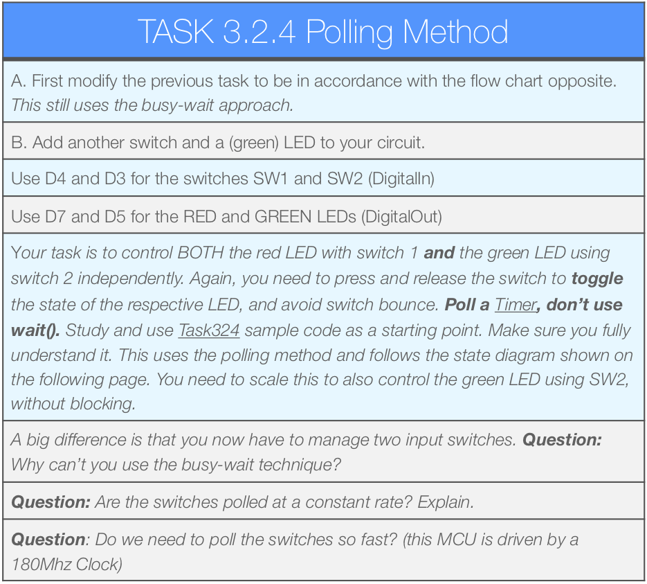
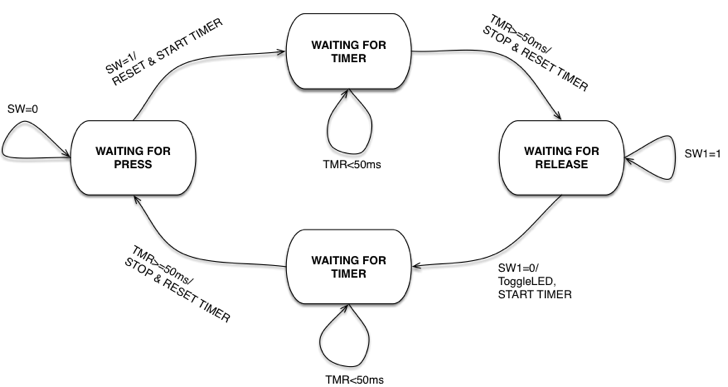
In the next task we implement such a methodology where we poll two devices: a timer and a switch. You should read the Mbed-os documentation for the Timer class before you attempt the next task. This is quite a tough (but important) task, so see the tips given below as well.
TIPS
For this task, each switch and timer combination can be seen as a separate finite state machine. The basic code for a single switch/timer can be found here https://os.mbed.com/teams/University-of-Plymouth-Stage-2-and-3/code/Task324/
Try and see the relationship between this code and the state diagram below. This is important
A solution is here: https://os.mbed.com/teams/University-of-Plymouth-Stage-2-and-3/code/Task324Solution/. Only look at this if you are completely stuck.
If you managed the task above, well done. I suggest you make a note of the solution for future reference. The software pattern is reusable for other similar tasks.
Self-Study Challenge: Finite State Machines in C
This might be a good time to review the code solution above and observe how the switch-case is used to implement a state machine. Maybe make notes in your log books on implementation of software state machines using a switch-case. The following task is designed to further test your own understanding
Self-Directed Task
Using the same hardware as above, write a new project to do the following:
- On power up, the Green LED should flash continuously at a rate of once a second (1Hz).
- Pressing SW1 should reduce the flashing rate (frequency)
- Pressing SW2 should increase the flashing rate
- Pressing SW1 and SW2 together should reset the frequency to 1Hz
- Take steps to avoid switch bounce for both switches. Poll a timer to check the time. Do not use
wait() - Use one state machine per switch / timer pair. Maybe show the tutor your state-diagram before you write the code.
Document this in your log book / notes. Include a state diagram. Remember that your state diagram has two inputs, a switch and a timer, although you won’t necessarily poll both in each state.
Tips:
State diagrams can be sketched on paper, photographed with a smartphone or tablet and inserted into your logbook. I recommend using document scanning facility in OneDrive (for Android and iOS) to make this much more seamless.
You are strongly advised to complete this task before the next lab session. Remember a taught module is 200Hrs. This should be approximately 16 hours / week
4Hrs / week lectures
4Hrs / week practicals
8+hrs/week self study
Advanced Task
The state machines above are Mealy Machines (outputs are changed on state-transitions). If you are really curious, can you re-write this task as a Moore Machine? Hint: Split the state machine into two distinct switch-case blocks, one for the next state and the next for the output.